Difference Between BJT and FET
BJT and FET are two fundamental types of semiconductor devices used in electronic circuits. Both transistors play crucial roles in amplification and signal processing within electronic systems. These devices are essential components in various electronic applications. Read on to learn more about the two transistors and how they differ from each other. Let’s dive in!
What is BJT?
A Bipolar Junction Transistor (BJT) is a semiconductor device that functions as an amplifier or a switch in electronic circuits. It consists of three layers of semiconductor material: the emitter, base, and collector. It operates by controlling the flow of charge carriers (electrons or holes) between these layers. When a small input current is applied at the base, the BJT can control a larger current between the emitter and collector.
There are two types of BJTs, namely NPN (negative-positive-negative) and PNP (positive-negative-positive), based on the doping types of the three main terminals. NPN transistors are more common, with electrons as charge carriers, while PNP transistors use holes as charge carriers.

What is FET?
A Field-Effect Transistor (FET) is a type of transistor used for amplification and switching in electronic circuits. Unlike a BJT, the FET operates based on an electric field. It has three terminals: source, gate, and drain. The flow of current between the source and drain is controlled by the voltage applied to the gate terminal.
FETs come in two primary types: Metal-Oxide-Semiconductor FET (MOSFET) and Junction FET (JFET). MOSFETs are prevalent in digital circuits, while JFETs are used in analog circuits. FETs are essential components in modern electronics, offering high input impedance and low power consumption.
Difference between BJT and FET
Control Mechanism
A BJT works when a small current at the base terminal controls the flow of current between the emitter and collector terminals. The amount of base current determines the amplification or switching behavior.
FETs manage current flow between the source and drain terminals by changing the voltage on the gate terminal. The gate voltage creates an electric field that adjusts the channel’s conductivity between the source and drain.
Charge Carriers
In NPN-type BJTs, electrons are the main charge carriers, while in PNP-type BJTs, holes (lack of electrons) are the majority carriers. Both types of carriers contribute to current flow in various transistor setups.
N-Channel FETs mainly use electrons as charge carriers, whereas P-Channel FETs use holes. This difference in charge carriers influences the direction of current flow in FETs.
Polarity
NPN BJTs have a structure of negative-positive-negative layers, while PNP BJTs have a positive-negative-positive arrangement. This polarity affects current flow direction and the types of charge carriers.
N-Channel FETs have an N-type semiconductor channel, and P-Channel FETs have a P-type channel. The choice of channel type determines the polarity and behavior of the FET.
Input Impedance
BJTs generally have lower input impedance compared to FETs. The input impedance of a transistor affects how much it loads the signal source. Lower input impedance can lead to greater signal source loading.
FETs exhibit high input impedance, making them suitable for applications where the signal source needs to be minimally loaded.
Voltage vs. Current Control
BJTs are primarily voltage-controlled devices. The voltage applied at the base-emitter junction controls the current flow between the collector and emitter. The input current at the base is transformed into a larger output current.
FETs are also voltage-controlled devices, and their operation depends on the voltage applied to the gate. FETs have high input impedance, meaning they draw minimal current from the input source.
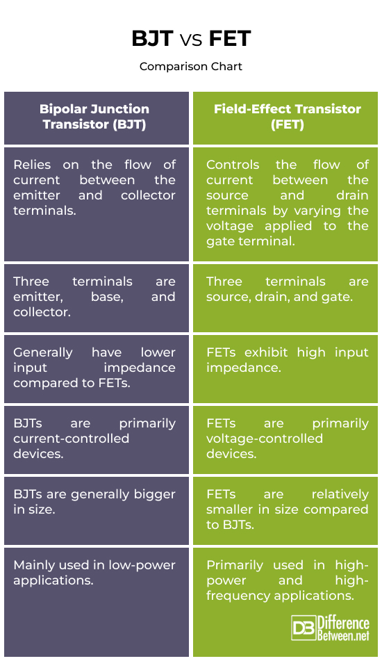
BJT vs. FET: Comparison Chart
Summary
Both transistors are crucial for amplification and signal processing in electronic systems. BJT focuses on controlling current, while FET emphasizes voltage control. BJT manages charge carriers’ flow between layers, and FET regulates charge carriers using an electric field. Understanding these differences is vital for selecting components in specific applications.
FAQs
What is the main difference between BJT and FET?
BJT controls current using a small current at the base, while FET controls current with a voltage applied to the gate.
What is the main advantage of FET over BJT?
FETs draw minimal current, reducing loading effects. This makes them suitable for applications where signal integrity is crucial.
Why is BJT faster than FET?
On the contrary, FETs are often considered faster than BJTs. FETs exhibit higher switching speeds and are preferred in high-frequency applications due to their reduced transition times.
Why use a FET instead of a transistor?
FETs are a type of transistor. The term “transistor” is a general category that includes both BJT and FET.
What is the major disadvantage of BJTs over FETs?
BJTs have lower input impedance than FETs, leading to higher loading effects on the signal source, impacting performance in circuits where signal integrity is crucial.
What is the main advantage of FET?
The main advantage of FETs is their high input impedance, which minimizes loading effects on the signal source. This makes FETs suitable for maintaining input signal integrity.
Can I use BJT instead of FET?
While BJTs and FETs share similarities, their distinct characteristics make them suitable for different scenarios.
Is a MOSFET faster than a BJT?
Generally, MOSFETs are considered faster than BJTs due to high switching speeds and low ON resistance.
Is a MOSFET just a relay?
No, a MOSFET is not just a relay. They serve as switches but operate on different principles. A MOSFET is a semiconductor device, whereas a relay is an electromagnetic switch that uses an electromagnet to control the flow of current.
- Difference Between Caucus and Primary - June 18, 2024
- Difference Between PPO and POS - May 30, 2024
- Difference Between RFID and NFC - May 28, 2024
Search DifferenceBetween.net :
23 Comments
Leave a Response
References :
[0]Cripps, Steve C. Advanced Techniques in RF Power Amplifier Design. Artech House, 2002.
[1]Tietze, Ulrich ,et al. Electronic Circuits: Handbook for Design and Application. Springer, 2015.
[2]Image credit: https://www.canva.com/photos/MADyRsNRdvU-broken-into-pieces-old-bipolar-transistor/
[3]Image credit: https://www.canva.com/photos/MAE2Fpoe5w0-transistor/
Thnx, very useful and resumed information
Thanks
Thnq veryy much 🙂
Thanx
thanxs
Tanx , for the tutorial ….
Thank U for help
hi, this is an awesome site for me in my study . Ttank u
tnx for help
very useful link
i thnk you should described it by table form..!!
tNx too loT
thanx a lot
tnx alot
tnx a lot…..vry hlpful site
tnx for help but it better if written in tabular form
Good your job sir. we grateful for this kind of ur opinion…..
Fanx alot
Thnx
Thank you
thanks
This are wonderful notes.Thanks so much…
Thanks a lot for this site
Thank you sir for this answer